Can You Use ESP32 as SWD Programmer for STM32 with Rust?
Build a simple SWD debug probe with an ESP32 and Rust. Learn how the ARM Serial Wire Debug protocol works, communicate with an STM32 Blue Pill, and read the target's Debug Port IDCODE. Yes. You can use an ESP32 as an SWD programmer for an STM32. In this tutorial, we implement the SWD protocol in Rust and use an ESP32 to communicate with an STM32F103C8T6 Blue Pill and read its DP IDCODE. In my next post, I will use it to actually program the STM32F103. I was browsing Reddit and came across someone asking how to program the STM32F103C8T6 without an ST-Link V2. They were asking whether it was possible to use an STM32F401RCT6 (Black Pill) board as an SWD programmer for an STM32F103C8T6 (Blue Pill). That post made me curious about how the SWD protocol works. Is it possible to build one myself? I did not have two STM32 boards at the time (I had broken my Black Pill in a different experiment). I had an ESP32 DevKit and a Blue Pill, along with other boards like the Pico. But I usually use a debug probe or another programmer with those boards. The ESP32 DevKit is the one where I can make fewer connections (since it does not require a debug probe), so I chose it for this experiment. SWD stands for Serial Wire Debug. It is a debug protocol developed by Arm Limited for communicating with and debugging Arm microcontrollers. Before SWD, JTAG was commonly used for debugging and programming microcontrollers. Compared to JTAG, SWD uses only two pins: Clock (SWCLK) and Data (SWDIO). We will use an ESP32 DevKit as the SWD programmer and an STM32F103C8T6 Blue Pill as the target. The ESP32 and Blue Pill are powered separately through their USB connections. We only need to connect the SWD signals and ground between them. SWD uses two signals: SWCLK and SWDIO. The host, which in our case is the ESP32, drives the SWCLK signal and uses the bidirectional SWDIO line to communicate with the target STM32. NOTE: A target can have multiple Access Ports (APs). This diagram shows a single AP for simplicity. The SWD interface connects to the Debug Port (DP). The DP handles communication with the host and provides access to one or more Access Ports (APs). An AP provides access to different parts of the target system. A SWD transfers data one bit at a time, with bits transmitted least significant bit (LSB) first. Now that we understand the basic SWD signals, we can implement them in Rust. We will start with the basic operations needed to read and write bits over the SWD interface. The SWCLK signal provides the timing for SWD communication. We can generate one clock cycle by driving SWCLK low and then high, with a short delay between each transition. Each call to Since SWDIO is a bidirectional signal, we will create the SWDIO pin as a To switch the pin between input and output, we will create two helper functions: To send a bit to the target, we first set SWDIO to the required logical level and then generate one clock cycle. As we learnt, the SWDIO level is sampled on the rising edge of SWCLK. We read the value just before driving SWCLK high so that we capture the bit for that clock cycle. So, we first drive SWCLK low. We then read the SWDIO level. Finally, we drive SWCLK high. Most of the time, we will need to read or write multiple bits as a whole, even though they are sent or received one by one. We will create convenient functions to handle reading and writing multiple bits. Because SWD transmits bits least significant bit (LSB) first, For reading, the first bit received becomes bit 0 of the returned value, the next bit becomes bit 1, and so on. Before we can communicate with the target using SWD, we need to switch the debug interface from JTAG to SWD. The ARM specification defines three steps for this: Once this is done, our SWD interface is ready for communication. First, we will create a helper function for the line reset: We send 52 clock cycles instead of the required 50 to provide a small margin. Now we can implement the JTAG-to-SWD switch: The first After the select sequence, we send another line reset. Finally, we keep SWDIO LOW and generate four clock cycles to leave the interface in the idle state. A typical SWD transaction has three phases: Because SWDIO is bidirectional, the host and target must take turns driving it. A one-cycle turnaround is inserted when control of SWDIO changes. During the turnaround cycle, neither side drives SWDIO. In our case, we will read the STM32’s DP An SWD request is an 8-bit packet sent by the host. It tells the target whether the host wants to access the Debug Port (DP) or an Access Port (AP), whether the operation is a read or write, and which register is being accessed. The request packet contains the following fields: Some of the fields are constant in the request. I will explain only the bits that we can change. APnDP This bit selects which port the request is sent to. A value of RnW This bit selects the type of operation. A value of Address Bits The Since we will be reading the The For our As it is obvious, the number of With the After the host sends the request, the target responds with a 3-bit ACK. The ACK tells the host whether the operation was successful. There are three possible ACK responses: If you saw the ACK table in the ARM specification, the values are reversed. For example, the specification shows We have now seen what an SWD transaction looks like. Let’s implement it step by step, starting with the request packet. First, we need to construct the 8-bit request packet that will be sent by the host. After sending the request, the target responds with a 3-bit ACK. We can create a helper function to read and interpret this response. Before reading the register, we need a small helper to put SWDIO into the idle state: We can now implement the function to read a register. Once we have that, we can create a small wrapper function specifically for reading the DP We first call the As you noticed, the After sending the request, we switch the SWDIO pin to input mode. Then we wait for one clock cycle to give control to the target. The target will now send the acknowledgment bits followed by the data bits. So, we first read the 3 acknowledgment bits. Then we read the next 32 bits as the We then calculate the expected parity from the received In the I have created If you have a logic analyzer, we can use it to see the SWD communication on the wire. You can check out my blog post on using a logic analyzer. PulseView also has an SWD decoder that you can use to decode the captured communication. The capture below shows the complete sequence: The clock does not look perfectly symmetric in the capture, but an exact 50% duty cycle is not required for SWD. What matters here is that the data is sampled on the rising edge of SWCLK. It Ain’t Much, But It’s Honest Work. I have not achieved the end goal yet: flashing the STM32 board with an ESP32. But this is the groundwork, and I believe I am on the right track. I am able to successfully communicate with the STM32 over SWD and read its You can find the complete project on GitHub. My next experiment is to flash the STM32. If I am successful and can fit everything into a blog post, you can read about it in my next blog post.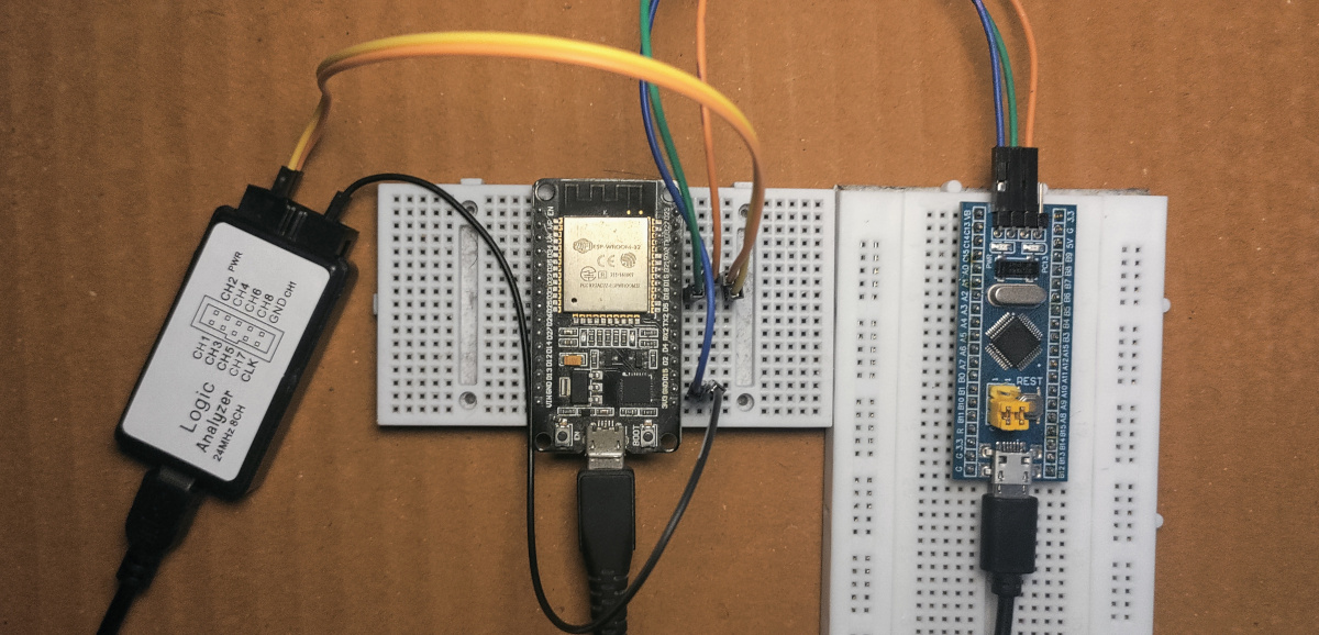
SWD
Hardware Setup
ESP32 Wire STM32 GPIO18 SWCLK (PA14) GPIO19 SWDIO (PA13) GND GND How Does SWD Work?
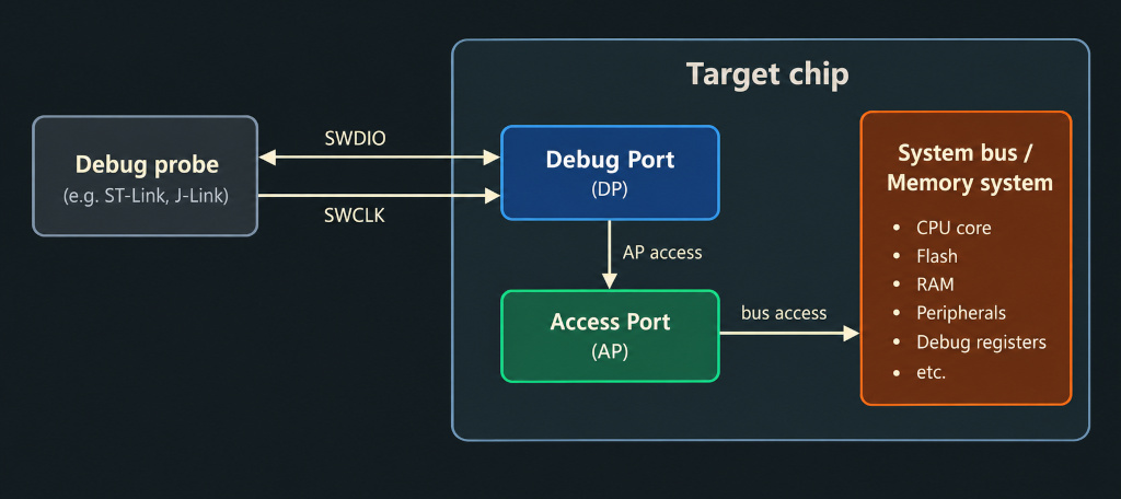
Understanding the SWD Protocol
high level on SWDIO represents a logical 1, while a low level represents a logical 0. The host and target sample the SWDIO signal on the rising edge of SWCLK when receiving data.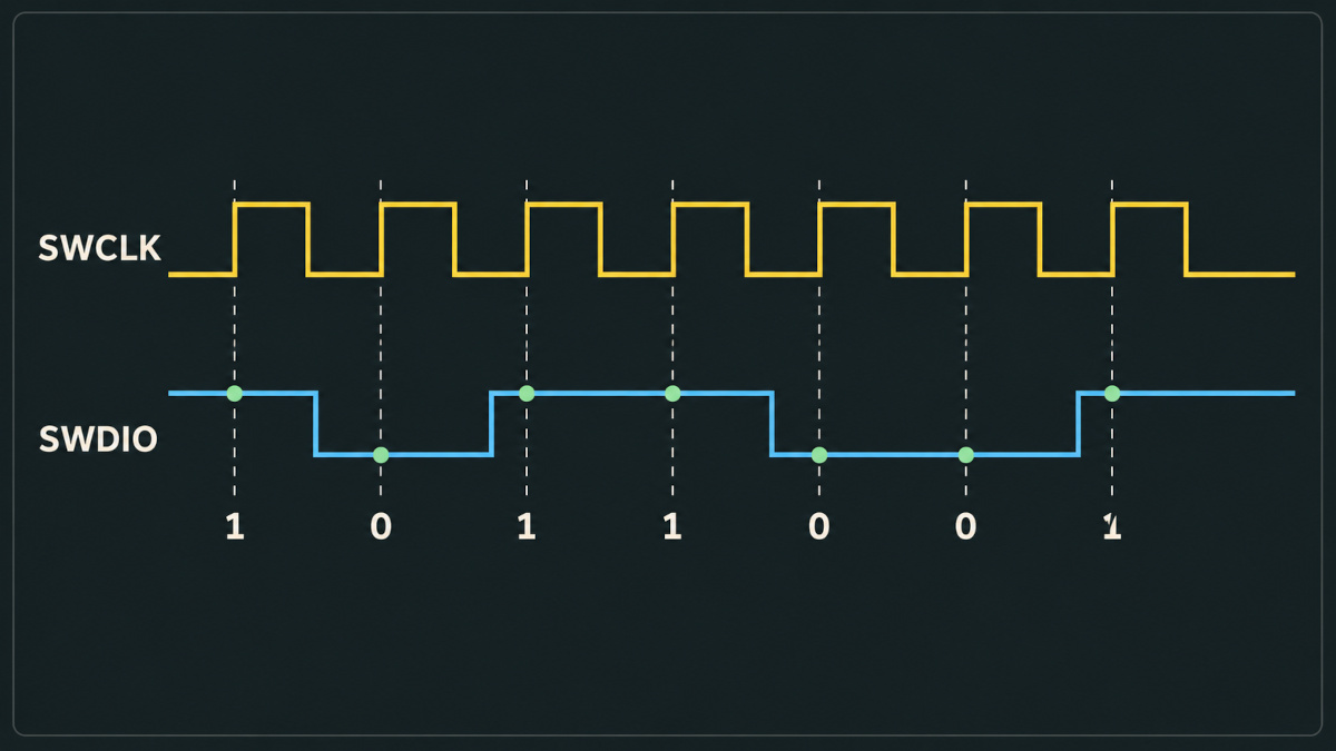
Implementing the SWD Signals in Rust
Generating the SWD Clock
fn clock(&mut self) {
    self.swclk.set_low();
    self.delay.delay_micros(1);

    self.swclk.set_high();
    self.delay.delay_micros(1);
}clock() generates one SWCLK cycle. Switching SWDIO Direction
Flex. This allows us to switch the pin between input and output.let swdio = Flex::new(peripherals.GPIO19);fn swdio_output(&mut self) {
self.swdio.set_input_enable(false);
self.swdio.set_output_enable(true);
}
fn swdio_input(&mut self) {
self.swdio.set_output_enable(false);
self.swdio.set_input_enable(true);
} Writing a Bit
fn write_bit(&mut self, bit: bool) {
if bit {
self.swdio.set_high();
} else {
self.swdio.set_low();
}
self.swclk.set_low();
self.delay.delay_micros(1);
self.swclk.set_high();
self.delay.delay_micros(1);
} Reading a Bit
fn read_bit(&mut self) -> bool {
self.swclk.set_low();
self.delay.delay_micros(1);
let bit = self.swdio.is_high();
self.swclk.set_high();
self.delay.delay_micros(1);
bit
} Reading and Writing Multiple Bits
write_bits() sends the least significant bit first and shifts the value right after each bit.fn write_bits(&mut self, mut value: u32, count: usize) {
for _ in 0..count {
self.write_bit((value & 1) != 0);
value >>= 1;
}
}fn read_bits(&mut self, count: usize) -> u32 {
let mut value = 0;
for bit in 0..count {
if self.read_bit() {
value |= 1 << bit;
}
}
value
} Switching from JTAG to SWD
0xE79E as bits.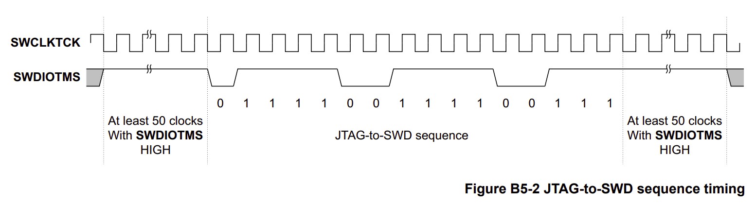
Implementation code for Switching from JTAG to SWD
fn line_reset(&mut self) {
self.swdio.set_high();
for _ in 0..52 {
self.clock();
}
}fn switch_to_swd(&mut self) {
// 1. Put the interface into reset state.
self.swdio_output();
self.line_reset();
// 2. JTAG -> SWD selection sequence.
// SWD transmits bits LSB first.
self.write_bits(0xE79E, 16);
// 3. Put the SWD interface into line reset state.
self.line_reset();
self.swdio.set_low();
// SWD requires at least 2 idle cycles
for _ in 0..4 {
self.clock();
}
}line_reset() sends the required clock cycles with SWDIO held HIGH. We then send the JTAG-to-SWD select sequence using 0xE79E. SWD Transaction
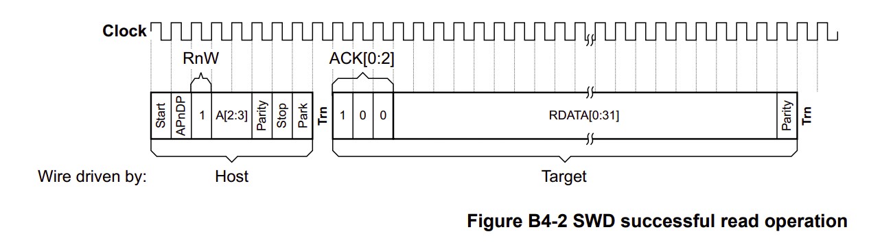
IDCODE. The IDCODE is a register in the Debug Port (DP) that contains identification information for the debug port. The host first sends a request to read the register. The target responds with an acknowledgment. The target then sends the 32-bit IDCODE followed by a parity bit. SWD Request Packet
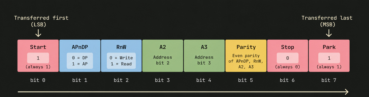
0 selects the Debug Port (DP), while a value of 1 selects an Access Port (AP). The DP provides access to the debug interface itself, while an AP provides access to resources such as the target’s memory system.0 selects a write, while a value of 1 selects a read.A2 and A3 bits are used to select the register address. The two lower address bits, A1 and A0, are not included in the request and are always 0. Together, A3 and A2 select one of four possible register offsets:A3 A2 Address DP register 0 0 0x00 IDCODE on read, ABORT on write 0 1 0x04 CTRL/STAT 1 0 0x08 RESEND on read, SELECT on write 1 1 0x0C RDBUFF on read IDCODE register, we use address 0x00. Parity
Parity bit is used to detect errors in the request. It is calculated from the APnDP, RnW, A2, and A3 bits. SWD uses even parity, which means the total number of 1 bits across these five bits must be even.IDCODE read request, APnDP will be 0 because we are accessing the DP, RnW will be 1 because we are performing a read, and the address will be 0x00, which is the address we saw earlier for IDCODE.APnDP = 0
RnW = 1
A2 = 0
A3 = 01 bits here is odd (only one). So, we have to set the Parity bit to 1 to make the total number of 1 bits even.Parity bit calculated, the complete request is transferred as follows: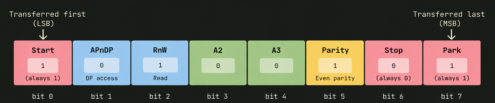
SWD ACK
ACK Response Meaning 0b001 OK The read or write operation was successful 0b010 WAIT The target is not ready to complete the read or write operation 0b100 FAULT The target detected a fault during the read or write operation 0b100 for OK. This is because it is showing the ACK[0:2] field in transfer order, with bit 0 first. Our program reads the bits in the order they arrive and constructs an integer value, so OK becomes 0b001. Implementing an SWD Transaction
Building the SWD Request
const START_BIT: u8 = 0b1;
const PARK_BIT: u8 = 0b1 << 7;
#[derive(Clone, Copy, PartialEq, Eq)]
enum Port {
Dp,
Ap,
}
#[derive(Clone, Copy, PartialEq, Eq)]
enum Access {
Read,
Write,
}
fn make_request(port: Port, access: Access, address: u8) -> u8 {
let ap = u8::from(port == Port::Ap);
let read = u8::from(access == Access::Read);
let a2 = (address >> 2) & 1;
let a3 = (address >> 3) & 1;
let parity = ap ^ read ^ a2 ^ a3;
START_BIT | (ap << 1) | (read << 2) | (a2 << 3) | (a3 << 4) | (parity << 5) | PARK_BIT
} Reading the ACK
const ACK_OK: u8 = 0b001;
const ACK_WAIT: u8 = 0b010;
const ACK_FAULT: u8 = 0b100;
fn read_ack(&mut self) -> Result<(), SwdError> {
match self.read_bits(3) as u8 {
ACK_OK => Ok(()),
ACK_WAIT => Err(SwdError::Wait),
ACK_FAULT => Err(SwdError::Fault),
ack => Err(SwdError::InvalidAck(ack)),
}
} Reading a Register
fn idle_cycle(&mut self) {
self.swdio_output();
self.swdio.set_low();
for _ in 0..2 {
self.clock();
}
}IDCODE.const DP_IDCODE: u8 = 0x00;
fn read_register(&mut self, port: Port, address: u8) -> Result<u32, SwdError> {
let request = Self::make_request(port, Access::Read, address);
self.swdio_output();
// Request.
self.write_bits(request as u32, 8);
// Turnaround.
self.swdio_input();
self.clock();
// ACK.
self.read_ack()?;
// Data.
let value = self.read_bits(32);
// Parity.
let parity = self.read_bit();
let expected_parity = (value.count_ones() & 1) != 0;
if parity != expected_parity {
return Err(SwdError::ParityError);
}
// Target -> host turnaround.
self.swdio_input();
self.clock();
// Host now owns SWDIO.
self.swdio_output();
self.idle_cycle();
Ok(value)
}
pub fn read_dp_idcode(&mut self) -> Result<u32, SwdError> {
self.read_register(Port::Dp, DP_IDCODE)
}make_request function with the port set to Dp, the access type set to Read, and the address of the IDCODE register, which is 0x00.make_request function does not send the request. It gives us the value that needs to be sent. We then put the SWDIO pin in output mode and write those bits.IDCODE. Finally, we read the parity bit.IDCODE and compare it with the parity bit we received. If they are different, it means the parity check failed, so we return a ParityError. If they match, we can return the received IDCODE. Putting It All Together
main function, we can now call the functions we created. The flow is simple: we switch the target to SWD and then read the DP IDCODE.Swd as a struct to keep all the SWD-related functionality together. You can check out the full code for the Swd struct.swd.switch_to_swd();
esp_println::println!("Reading DP IDCODE...");
match swd.read_dp_idcode() {
Ok(idcode) => {
esp_println::println!("SWD connected!");
esp_println::println!("DP IDCODE = {:#010x}", idcode);
}
Err(error) => {
defmt::error!("SWD error: {}", error);
}
} Verifying with a Logic Analyzer

Final Thoughts
IDCODE. Full Code
#![no_std]
#![no_main]
#![deny(
clippy::mem_forget,
reason = "mem::forget is generally not safe to do with esp_hal types, especially those \
holding buffers for the duration of a data transfer."
)]
#![deny(clippy::large_stack_frames)]
use defmt::error;
use esp_hal::clock::CpuClock;
use esp_hal::delay::Delay;
use esp_hal::gpio::{Flex, Level, Output, OutputConfig};
use esp_hal::main;
use esp_println as _;
#[panic_handler]
fn panic(panic_info: &core::panic::PanicInfo) -> ! {
error!("{}", panic_info);
loop {}
}
esp_bootloader_esp_idf::esp_app_desc!();
const ACK_OK: u8 = 0b001;
const ACK_WAIT: u8 = 0b010;
const ACK_FAULT: u8 = 0b100;
const START_BIT: u8 = 0b1;
const PARK_BIT: u8 = 0b1 << 7;
const DP_IDCODE: u8 = 0x00;
#[derive(Clone, Copy, PartialEq, Eq)]
enum Port {
Dp,
Ap,
}
#[derive(Clone, Copy, PartialEq, Eq)]
enum Access {
Read,
#[allow(dead_code)]
Write, // Will use later
}
struct Swd<'d> {
swclk: Output<'d>,
swdio: Flex<'d>,
delay: Delay,
}
#[derive(defmt::Format)]
enum SwdError {
Wait,
Fault,
InvalidAck(u8),
ParityError,
}
impl<'d> Swd<'d> {
fn new(swclk: Output<'d>, mut swdio: Flex<'d>, delay: Delay) -> Self {
swdio.set_input_enable(false);
swdio.set_output_enable(true);
swdio.set_low();
Self {
swclk,
swdio,
delay,
}
}
fn clock(&mut self) {
self.swclk.set_low();
self.delay.delay_micros(1);
self.swclk.set_high();
self.delay.delay_micros(1);
}
fn read_bit(&mut self) -> bool {
self.swclk.set_low();
self.delay.delay_micros(1);
let bit = self.swdio.is_high();
self.swclk.set_high();
self.delay.delay_micros(1);
bit
}
fn read_bits(&mut self, count: usize) -> u32 {
let mut value = 0;
for bit in 0..count {
if self.read_bit() {
value |= 1 << bit;
}
}
value
}
fn write_bit(&mut self, bit: bool) {
if bit {
self.swdio.set_high();
} else {
self.swdio.set_low();
}
self.clock();
}
fn write_bits(&mut self, mut value: u32, count: usize) {
for _ in 0..count {
self.write_bit((value & 1) != 0);
value >>= 1;
}
}
fn swdio_output(&mut self) {
    self.swdio.set_input_enable(false);
    self.swdio.set_output_enable(true);
}

fn swdio_input(&mut self) {
    self.swdio.set_output_enable(false);
    self.swdio.set_input_enable(true);
}
fn line_reset(&mut self) {
    self.swdio.set_high();
    for _ in 0..52 {
        self.clock();
    }
}
fn switch_to_swd(&mut self) {
    // 1. Put the interface into reset state.
    self.swdio_output();

    self.line_reset();

    // 2. JTAG -> SWD selection sequence.
    // SWD transmits bits LSB first.
    self.write_bits(0xE79E, 16);

    // 3. Put the SWD interface into line reset state.
    self.line_reset();

    self.swdio.set_low();

    // SWD requires at least 2 idle cycles
    for _ in 0..4 {
        self.clock();
    }
}
fn make_request(port: Port, access: Access, address: u8) -> u8 {
let ap = u8::from(port == Port::Ap);
let read = u8::from(access == Access::Read);
let a2 = (address >> 2) & 1;
let a3 = (address >> 3) & 1;
let parity = ap ^ read ^ a2 ^ a3;
START_BIT | (ap << 1) | (read << 2) | (a2 << 3) | (a3 << 4) | (parity << 5) | PARK_BIT
}
fn read_ack(&mut self) -> Result<(), SwdError> {
match self.read_bits(3) as u8 {
ACK_OK => Ok(()),
ACK_WAIT => Err(SwdError::Wait),
ACK_FAULT => Err(SwdError::Fault),
ack => Err(SwdError::InvalidAck(ack)),
}
}
fn idle_cycle(&mut self) {
    self.swdio_output();
    self.swdio.set_low();

    for _ in 0..2 {
        self.clock();
    }
}
fn read_register(&mut self, port: Port, address: u8) -> Result<u32, SwdError> {
let request = Self::make_request(port, Access::Read, address);
self.swdio_output();
// Request.
self.write_bits(request as u32, 8);
// Turnaround.
self.swdio_input();
self.clock();
// ACK.
self.read_ack()?;
// Data.
let value = self.read_bits(32);
// Parity.
let parity = self.read_bit();
let expected_parity = (value.count_ones() & 1) != 0;
if parity != expected_parity {
return Err(SwdError::ParityError);
}
// Target -> host turnaround.
self.swdio_input();
self.clock();
// Host now owns SWDIO.
self.swdio_output();
self.idle_cycle();
Ok(value)
}
pub fn read_dp_idcode(&mut self) -> Result<u32, SwdError> {
self.read_register(Port::Dp, DP_IDCODE)
}
}
#[allow(
clippy::large_stack_frames,
reason = "it's not unusual to allocate larger buffers etc. in main"
)]
#[main]
fn main() -> ! {
let config = esp_hal::Config::default().with_cpu_clock(CpuClock::max());
let peripherals = esp_hal::init(config);
let delay = Delay::new();
let swclk = Output::new(peripherals.GPIO18, Level::Low, OutputConfig::default());
let swdio = Flex::new(peripherals.GPIO19);
let mut swd = Swd::new(swclk, swdio, delay);
swd.switch_to_swd();

esp_println::println!("Reading DP IDCODE...");

match swd.read_dp_idcode() {
    Ok(idcode) => {
        esp_println::println!("SWD connected!");

        esp_println::println!("DP IDCODE = {:#010x}", idcode);
    }

    Err(error) => {
        defmt::error!("SWD error: {}", error);
    }
}
loop {
core::hint::spin_loop();
}
} Reference