Flashing STM32 Firmware with ESP32 and Embedded Rust
Flash firmware to an STM32 Blue Pill using an ESP32 and Embedded Rust. Learn how to access STM32 memory through the SWD AHB Access Port, unlock and erase Flash, program firmware, and verify the written data. If you have read my previous articles, you know that I started with the goal of writing Embedded Rust code to use an ESP32 DevKit as a programmer and flash firmware into an STM32 Blue Pill board(STM32F103C8T6). You can check out my previous articles: Now, we have the foundation in place. We can finally implement a simple program to flash firmware to the STM32. The overall flow is: You can check out the completed project here and cross-reference the code to see how everything fits together in the final program. The program we are going to flash into the STM32 is a simple LED blinky program. You can find the source code for this blinky program here. You need to generate a binary file from the program you want to flash: You can then copy this binary into our project. Now that we are able to talk to the AHB Access Port, we can access the STM32 system through it, including Flash, SRAM, memory-mapped peripheral registers, and processor registers. This access is independent of the processor’s status. To access the STM32 memory through the AHB Access Port, we need to use two registers: the Transfer Address Register (TAR) and the Data Read/Write Register (DRW). The TAR register holds the address in the STM32 memory that we want to access. The DRW register is used to read data from or write data to that address. For example, to write a value to a memory address, we first write the address to TAR and then write the value to DRW. To read from a memory address, we first write the address to TAR and then read the data from DRW. We can wrap these operations in two helper functions: Before we can perform memory transfers, we need to configure how the AHB Access Port should access memory. For example, we need to specify whether each transfer should be 16 or 32 bits. The AHB-AP uses the Control and Status Word (CSW) register for this configuration. I will not cover all the fields in the CSW register here. You can refer to the Cortex-M3 Technical Reference Manual for the complete description. For our purposes, we mainly focus on the The The second field we are interested in is So, the typical CSW register value for a 32-bit transfer is We will create two helper functions to access the STM32 memory. They will set the CSW register for 32-bit access and then use the TAR and DRW registers to write to or read from the target address. Before writing a new program to Flash, we first halt the CPU. This prevents the processor from executing instructions while we modify the Flash contents. To achieve this, we use the Cortex-M3’s Debug Halting Control and Status Register (DHCSR). This is a memory-mapped debug register located at address The three bits we care about are We must write We will use the Everything is ready for our flashing procedure. We need to follow the procedure described in the STM32 PM0075 programming manual. Overall, we need to unlock the Flash controller, erase the required Flash pages, program the firmware, verify the programmed image, and lock the Flash controller again. Before programming the Flash, it is useful to understand how the Flash memory is organized. The PM0075 programming manual describes the Flash module organization in Section 1.2, including how the Flash memory is divided into pages. I will not go into the Flash organization in detail here. For our programmer, the important details are that the STM32F103C8T6 has To unlock the controller, we have to write two keys into the According to the PM0075 programming manual, the internal RC oscillator (HSI) must be enabled for Flash write and erase operations. The RM0008 reference manual describes the RCC registers used to control the clock. The HSI RC oscillator can be enabled using the Before and after Flash operations, we need to check the status of the Flash controller. The The We first determine which Flash pages are needed for the firmware image. We then erase each of those pages one by one. The The STM32F1 Flash memory is programmed one half-word (16-bit) at a time. Therefore, the AHB-AP must be configured for a The AHB-AP For a half-word transfer, the specification uses We will place the value in the lower 16 bits for addresses ending in We can now put the firmware into Flash. We enable Flash programming by setting the After each write, we wait for the Flash operation to complete and check the status for errors. Once the entire image has been programmed, we clear the The After programming the firmware, we read the Flash memory back and compare it with the original image. We read After programming and verifying the firmware, we lock the Flash controller again by setting the After flashing the firmware, we need to reset the system. The Application Interrupt and Reset Control Register (AIRCR) is located at To request a system reset, we write Once done, you will want to run the core again. When I first tried flashing the firmware without the halt and run core functionality, I was wondering why the STM32 was not blinking. When I unplugged and plugged the USB back in, it started working. But then I realized that a better approach is to run the core once we flash the firmware. We can now put all the steps together to erase, program, and verify the Flash, then restart the core. It was a fun experiment and a nice to learn about SWD and the concepts around it. I would not say it was particularly hard or easy. The challenging part was figuring out which document to refer to. There is no single document that covers everything, so I had to refer to multiple documents along the way. Without the help of the Silicon Labs’ simplified guide and the QcentLabs blog post, it would have been much tougher to put everything together. I am not going to continue developing this programmer for now because I still have the LiteWing drone to play with and a few other side projects waiting for me. :P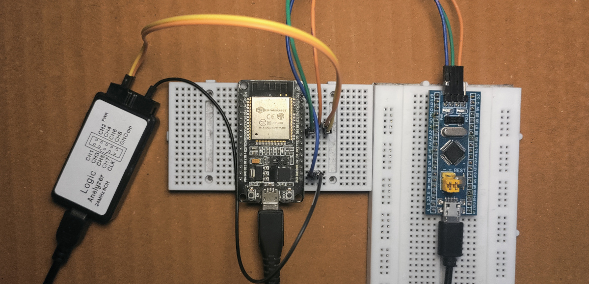
Plan
[Already Done] Connect to the STM32 through SWD and power up the debug system.[Already Done] Access the STM32 memory through the AHB Access Port. STM32 Firmware
cargo objcopy --release -- -O binary firmware.bin Accessing STM32 Memory
pub fn write_mem_ap(&mut self, address: u32, value: u32) -> Result<(), SwdError> {
    self.write_ap(AhbApRegister::Tar, address)?;
    self.write_ap(AhbApRegister::Drw, value)
}

pub fn read_mem_ap(&mut self, address: u32) -> Result<u32, SwdError> {
    self.write_ap(AhbApRegister::Tar, address)?;
    self.read_ap(AhbApRegister::Drw)
}
Configuring Memory Access
AddrInc and Size fields.AddrInc field controls whether the address is automatically incremented after a transfer. We will set it to 00, which disables automatic address incrementing.Size, which controls the size of the transfer. 001 selects a 16-bit transfer, while 010 selects a 32-bit transfer.0x2300_0042 for 32 Bit Size.jpg)
// 32-bit
const AHB_AP_CSW_32: u32 = 0x2300_0042;

// 16-bit
const AHB_AP_CSW_16: u32 = 0x2300_0041;
Reading and Writing Memory
// these functions goes into Stm32F1 struct

fn write_mem32(&mut self, address: u32, value: u32) -> Result<(), SwdError> {
    self.swd.write_ap(AhbApRegister::Csw, AHB_AP_CSW_32)?;
    self.swd.write_mem_ap(address, value)?;

    Ok(())
}

fn read_mem32(&mut self, address: u32) -> Result<u32, SwdError> {
    self.swd.write_ap(AhbApRegister::Csw, AHB_AP_CSW_32)?;
    self.swd.read_mem_ap(address)
}
Halting the Core
0xE000_EDF0. You can find more details about the DHCSR in the Armv7-M Architecture Reference Manual.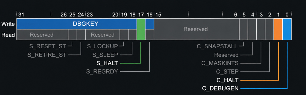
C_DEBUGEN, C_HALT, and S_HALT. The C_DEBUGEN bit enables debug access to the processor, allowing the debugger to halt and control its execution. Once debug access is enabled, setting C_HALT to 1 halts the processor, while clearing it to 0 allows the processor to resume execution.0xA05F to the Debug Key field in the upper 16 bits when writing to the lower 16 bits of the register. Otherwise, the processor ignores the write access.S_HALT bit to check whether the processor has been halted.const DHCSR: u32 = 0xE000_EDF0;
const DHCSR_DBGKEY: u32 = 0xA05F_0000;
const DHCSR_C_DEBUGEN: u32 = 1 << 0;
const DHCSR_C_HALT: u32 = 1 << 1;
const DHCSR_S_HALT: u32 = 1 << 17;
pub fn halt_core(&mut self) -> Result<(), SwdError> {
self.write_mem32(DHCSR, DHCSR_DBGKEY | DHCSR_C_DEBUGEN | DHCSR_C_HALT)?;
for _ in 0..100 {
let dhcsr = self.read_mem32(DHCSR)?;
if dhcsr & DHCSR_S_HALT != 0 {
return Ok(());
}
self.swd.delay.delay_micros(10);
}
Err(SwdError::HaltTimeout)
} Programming Procedure
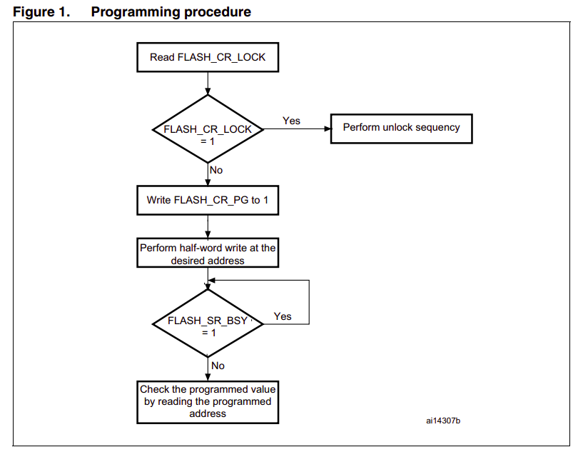
Flash Memory Organization
64 KB of Flash memory starting at 0x0800_0000, organized into 1 KB pages. A page is a fixed-size block of Flash memory that can be erased as a unit. Unlocking the Flash Controller
FLASH_KEYR register one by one. We can check whether the Flash controller is locked or not by checking the LOCK bit in the FLASH_CR register.const FLASH_BASE: u32 = 0x0800_0000;
const FLASH_REG_BASE: u32 = 0x4002_2000;
const FLASH_KEYR: u32 = FLASH_REG_BASE + 0x04;
const FLASH_CR: u32 = FLASH_REG_BASE + 0x10;
// Flash memory Program/Erase Controller(FPEC) unlock keys.
const FLASH_KEY1: u32 = 0x4567_0123;
const FLASH_KEY2: u32 = 0xCDEF_89AB;
const FLASH_CR_LOCK: u32 = 1 << 7;
pub fn flash_unlock(&mut self) -> Result<(), SwdError> {
let cr = self.read_mem32(FLASH_CR)?;
if cr & FLASH_CR_LOCK == 0 {
return Ok(());
}
self.write_mem32(FLASH_KEYR, FLASH_KEY1)?;
self.write_mem32(FLASH_KEYR, FLASH_KEY2)?;
let cr = self.read_mem32(FLASH_CR)?;
if cr & FLASH_CR_LOCK != 0 {
return Err(SwdError::FlashError(cr));
}
Ok(())
} Enabling the HSI Oscillator
HSION bit in the RCC_CR register. We can check the HSIRDY bit to determine whether the oscillator is stable and ready to use.const RCC_CR: u32 = 0x4002_1000;
const RCC_CR_HSION: u32 = 1 << 0;
const RCC_CR_HSIRDY: u32 = 1 << 1;
fn ensure_hsi_on(&mut self) -> Result<(), SwdError> {
let cr = self.read_mem32(RCC_CR)?;
if cr & RCC_CR_HSIRDY != 0 {
// Already on and stable.
return Ok(());
}
self.write_mem32(RCC_CR, cr | RCC_CR_HSION)?;
for _ in 0..1000 {
if self.read_mem32(RCC_CR)? & RCC_CR_HSIRDY != 0 {
return Ok(());
}
self.swd.delay.delay_micros(10);
}
Err(SwdError::FlashTimeout)
} Flash Status Flags
BSY bit in the FLASH_SR register indicates whether a Flash operation is still in progress. We wait until this bit is cleared before continuing.PGERR and WRPRTERR bits indicate programming and write-protection errors. The EOP(End of the Program) bit indicates that a Flash operation has completed successfully. We also clear these status flags before starting a new Flash operation.const FLASH_SR: u32 = FLASH_REG_BASE + 0x0C;
const FLASH_SR_BSY: u32 = 1 << 0;
const FLASH_SR_PGERR: u32 = 1 << 2;
const FLASH_SR_WRPRTERR: u32 = 1 << 4;
const FLASH_SR_EOP: u32 = 1 << 5;
fn flash_wait(&mut self) -> Result<u32, SwdError> {
for _ in 0..100_000 {
let status = self.read_mem32(FLASH_SR)?;
if status & FLASH_SR_BSY == 0 {
return Ok(status);
}
self.swd.delay.delay_micros(10);
}
Err(SwdError::FlashTimeout)
}
fn flash_check_status(&mut self, status: u32) -> Result<(), SwdError> {
let errors = status & (FLASH_SR_PGERR | FLASH_SR_WRPRTERR);
if errors != 0 {
return Err(SwdError::FlashError(status));
}
Ok(())
}
fn flash_clear_status(&mut self) -> Result<(), SwdError> {
self.write_mem32(FLASH_SR, FLASH_SR_EOP | FLASH_SR_PGERR | FLASH_SR_WRPRTERR)
} Erasing Flash Pages
const FLASH_PAGE_SIZE: u32 = 1024;
const FLASH_SIZE: u32 = 64 * 1024;

pub fn erase_for_image(&mut self, image_len: usize) -> Result<(), SwdError> {
    if image_len == 0 {
        return Ok(());
    }

    let image_len = image_len as u32;

    if image_len > FLASH_SIZE {
        return Err(SwdError::FirmwareTooLarge);
    }

    self.ensure_hsi_on()?;
    self.flash_wait()?;
    self.flash_clear_status()?;

    let last_address = FLASH_BASE + image_len - 1;

    let mut page = FLASH_BASE;

    while page <= last_address {
        self.flash_erase_page(page)?;

        page += FLASH_PAGE_SIZE;
    }

    Ok(())
}flash_erase_page function performs the actual page erase. The PER bit in the FLASH_CR register enables page erase. We select the page to erase by writing its address to FLASH_AR, then set the STRT bit to start the erase operation.const FLASH_AR: u32 = FLASH_REG_BASE + 0x14;
const FLASH_CR_PER: u32 = 1 << 1;
const FLASH_CR_STRT: u32 = 1 << 6;
fn flash_erase_page(&mut self, address: u32) -> Result<(), SwdError> {
// Make sure no previous operation is running.
self.flash_wait()?;
// PER = page erase.
self.write_mem32(FLASH_CR, FLASH_CR_PER)?;
// Select page.
self.write_mem32(FLASH_AR, address)?;
// Start erase.
self.write_mem32(FLASH_CR, FLASH_CR_PER | FLASH_CR_STRT)?;
let status = self.flash_wait()?;
self.flash_check_status(status)?;
// Clear PER after the operation.
let cr = self.read_mem32(FLASH_CR)?;
self.write_mem32(FLASH_CR, cr & !FLASH_CR_PER)?;
Ok(())
} Writing a Half-Word
16-bit access before writing the value.DRW register is 32 bits wide. It uses different parts of the DRW register depending on the transfer size and the address, so we place the half-word in the appropriate half of the register based on the address.fn write_mem16(&mut self, address: u32, value: u16) -> Result<(), SwdError> {
self.swd.write_ap(AhbApRegister::Csw, AHB_AP_CSW_16)?;
let value = if address & 0x2 == 0 {
value as u32
} else {
// lowest two bits of the target address are `10`
(value as u32) << 16
};
self.swd.write_mem_ap(address, value)
}DRW[15:0] when the address ends in 00, and DRW[31:16] when the address ends in 10.00, and shift it into the upper 16 bits for addresses ending in 10. Flashing the Firmware
PG bit in the FLASH_CR register. The firmware image is then written one half-word at a time using the write_mem16 function.PG bit.const FLASH_CR_PG: u32 = 1 << 0;
pub fn flash_program(&mut self, image: &[u8]) -> Result<(), SwdError> {
if !image.len().is_multiple_of(2) {
return Err(SwdError::FirmwareNotAligned);
}
self.ensure_hsi_on()?;
self.flash_wait()?;
self.flash_clear_status()?;
self.write_mem32(FLASH_CR, FLASH_CR_PG)?;
let result = self.program_procedure(image);
let cr = self.read_mem32(FLASH_CR)?;
self.write_mem32(FLASH_CR, cr & !FLASH_CR_PG)?;
result
}program_procedure function converts each pair of bytes into a 16-bit value and writes it to the next Flash address:fn program_procedure(&mut self, image: &[u8]) -> Result<(), SwdError> {
let mut index = 0;
let mut address = FLASH_BASE;
while index < image.len() {
let value = u16::from_le_bytes([image[index], image[index + 1]]);
self.write_mem16(address, value)?;
let status = self.flash_wait()?;
self.flash_check_status(status)?;
address += 2;
index += 2;
}
Ok(())
} Verifying the Firmware
32 bits at a time and compare each byte with the corresponding byte in the firmware image. If any byte differs, we return a VerifyFailed error with the address and the expected and actual values.pub fn verify_image(&mut self, image: &[u8]) -> Result<(), SwdError> {
let mut address = FLASH_BASE;
let mut index = 0;
while index < image.len() {
let value = self.read_mem32(address)?;
let bytes = value.to_le_bytes();
let count = (image.len() - index).min(4);
for offset in 0..count {
if bytes[offset] != image[index + offset] {
return Err(SwdError::VerifyFailed {
address: address + offset as u32,
expected: image[index + offset],
actual: bytes[offset],
});
}
}
address += 4;
index += count;
}
Ok(())
} Locking the Flash Controller
LOCK bit in the FLASH_CR register.pub fn flash_lock(&mut self) -> Result<(), SwdError> {
self.write_mem32(FLASH_CR, FLASH_CR_LOCK)
} Resetting the Core
0xE000_ED0C.0x5FA to the VECTKEY field and set the SYSRESETREQ bit to 1. This requests a reset of the system while leaving the debug system unaffected.const AIRCR: u32 = 0xE000_ED0C;
const AIRCR_VECTKEY: u32 = 0x5FA << 16;
const AIRCR_SYSRESETREQ: u32 = 1 << 2;
pub fn system_reset(&mut self) -> Result<(), SwdError> {
self.write_mem32(AIRCR, AIRCR_VECTKEY | AIRCR_SYSRESETREQ)?;
self.swd.delay.delay_millis(10);
Ok(())
}pub fn run_core(&mut self) -> Result<(), SwdError> {
self.write_mem32(DHCSR, DHCSR_DBGKEY | DHCSR_C_DEBUGEN)?;
Ok(())
} Putting It All Together
const FIRMWARE: &[u8] = {
    let bytes = include_bytes!("../../firmware.bin");

    assert!(!bytes.is_empty(), "Firmware image is empty.");
    assert!(bytes.len().is_multiple_of(2), "Firmware size must be even.");

    bytes
};

let swd = Swd::new(swclk, swdio, delay);
let mut stm32 = Stm32F1::new(swd);

// --------------------------------------------------------
// Connect to STM32
// --------------------------------------------------------

defmt::info!("Connecting to STM32...");

stm32
    .connect()
    .unwrap_or_else(|e| fail("STM32 connection failed", e));

defmt::info!("SWD connected!");

defmt::info!("Halting core...");
stm32
    .halt_core()
    .unwrap_or_else(|e| fail("Core halt failed", e));

// --------------------------------------------------------
// Unlock Flash
// --------------------------------------------------------

defmt::info!("Unlocking Flash...");

stm32
    .flash_unlock()
    .unwrap_or_else(|e| fail("Flash unlock failed", e));

defmt::info!("Flash unlocked.");

// --------------------------------------------------------
// Erase
// --------------------------------------------------------

defmt::info!("Erasing Flash...");

if let Err(error) = stm32.erase_for_image(FIRMWARE.len()) {
    let _ = stm32.flash_lock();

    fail("Flash erase failed", error);
}

defmt::info!("Flash erase complete.");

// --------------------------------------------------------
// Program
// --------------------------------------------------------

defmt::info!("Programming Flash...");

if let Err(error) = stm32.flash_program(FIRMWARE) {
    let _ = stm32.flash_lock();

    fail("Flash programming failed", error);
}

defmt::info!("Programming complete.");

// --------------------------------------------------------
// Verify
// --------------------------------------------------------

defmt::info!("Verifying Flash...");

if let Err(error) = stm32.verify_image(FIRMWARE) {
    let _ = stm32.flash_lock();

    fail("Verification failed", error);
}

defmt::info!("Verification successful!");

// --------------------------------------------------------
// Lock Flash
// --------------------------------------------------------

defmt::info!("Locking Flash...");

stm32
    .flash_lock()
    .unwrap_or_else(|e| fail("Flash lock failed", e));

defmt::info!("Flash locked.");

defmt::info!("Resetting STM32...");
stm32
    .system_reset()
    .unwrap_or_else(|e| fail("System reset failed", e));

defmt::info!("Running STM32...");
stm32
    .run_core()
    .unwrap_or_else(|e| fail("Core run failed", e));
Final Thoughts
References
Helpful Tutorials
Docs